Timur Nurmamytov
 Growth of ordered NW arrays containing magnetic inserts
Istituto Officina dei Materiali (CNR Trieste)
Scope of my project is the growth of ordered arrays of semiconductor nanowires (NWs) incorporating sections of magnetic materials, for innovative spintronic and nanophotonic devices. The integration of magnetic materials, either in the form of diluted magnetic semiconductors (e.g. GaMnAs) or magnetic metals (e.g. MnAs) in III-As NWs allow to add spintronic capabilities to electronic nanodevices. Besides, MnAs nanoparticles in GaAs NWs are interesting in view of their magneto-plasmonic activity.
The NWs will be grown as ordered arrays to produce the ensembles of identical nanowires. This is a major requirement for the implementation of multiple-wire devices on as grown samples. The use of arrays of the identical NWs allow to use “ensemble” characterisation techniques and obtain information representative of the “single” nanostructure. In addition, this opens the way to experiments using high “impact” techniques, (e.g. FEL radiation), that require a set of identical samples, due to the fact that the samples are destroyed during the measurement.
The main activities of project will involve the preparation of patterns by nanofabrication techniques, the growth of NWs using the molecular beam epitaxy (MBE) method and characterisation of the samples by microscopy and spectroscopy. The activities take place in “Istituto Officina dei Materiali” (IOM) of the Italian National Research Council (CNR), utilizing the multi-chamber ultra-high vacuum (UHV) system with two MBE growth chambers, a chamber for metal deposition and an analysis chamber for x-ray photoemission spectroscopy (XPS).
The patterning of samples will be done by nanoimprint lithography since it enables fast and relatively inexpensive processing. Meanwhile, the growth of GaAs NWs will be executed by solid source MBE on the patterned substrates for the optimization of process. The magnetic inclusions will be inserted in the form of 0-D MnAs (dots) and quasi 1-D nanostructures in the core-shell scheme. To tailor the size of magnetic portion, the recently demonstrated possibility of stopping and resuming the Ga-assisted growth of the NW by nucleating a new Ga nanoparticle at the tip of NW crystallization of the original one [Cryst.Growth & Des. 2013, 13, 3976] will be extensively exploited.

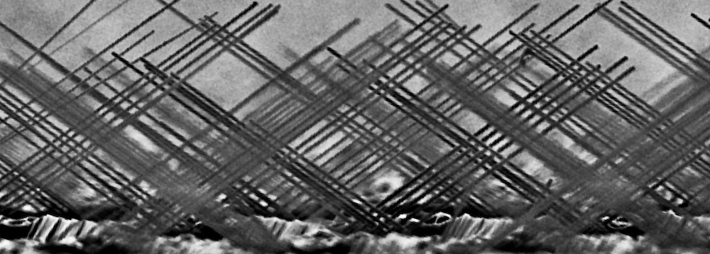
Fig.1 From left to right, GaAs NWs were the Ga nanoparticle has been crystallised, stopping the NW growth, and nucleated again, resuming the NW growth.
For the analysis of samples, the scanning electron microscopy (SEM) will be widely employed for morphological and chemical composition characterisation. The transmission electron microscopy and the Raman spectroscopy will be applied for the investigation of sample structure. Additionally, the magnetic properties of diluted GaAs will be studied by Magneto Optic Kerr Effect (MOKE) and synchrotron based x-ray measurements. Besides, the topic will be developed in close collaboration with IMM-CNR laboratory in Rome (a member of INDEED) where the optical studies will be completed.